Lab 1: First lab in the logic world
Objectives:
The purpose of the first lab is to be familiar with:
- The kit
- The breadboard
- How to use the Leds
- How to use the 7 segment display
- How to use switches to represent Binary numbers
- What is IC (Integrated circuits)
- How to connect any IC on the kit
- Push Buttons
Steps:
- Make sure that the power is on
- Get to know the boards can be used and which points are connected with each other.
- How to provide VCC & GND to the circuits.
- What is a LED (light Emitting Diode)
- How to use switches to represent Binary numbers
- Use the seven segment display to display binary numbers (0-9)
7447 BCD to 7-Segment Smart Simulator
Experiment with 4 digital switches to see how a real 7447 BCD-to-7-segment decoder drives a display. Toggle the switches to set a 4-bit BCD value (A: MSB, D: LSB). LEDs and segment output update instantly. Only valid BCD (0–9) is shown.
Lab 2: Implementing Basic Logic Gates
Objective:
Becoming familiar with the AND, OR and NOT (Inverter) logic operations implemented with TTL level integrated circuit gates.
Experiment requirements:
This experiment uses the following TTL level ICs; the pin configurations for these ICs are available in appendix A:
Procedure:
- Verify the truth table of logic gates by trying different combinations of inputs of the following gates:
AND, OR, NAND, NOR, XOR, XNOR, 3-input NAND, 4-input NAND - Implement the function of the NAND gate using AND gate & an INVERTER.
- Implement the function of the NAND gate using OR gate & an INVERTER.
- Using only one NAND gate, implement the function of a NOT gate.
- Using only one NOR gate, implement the function of a NOT gate.
Pre-lab Activity:
1. Fill the following truth tables for: AND, OR, NAND, NOR, XOR, XNOR
| A | B | AND | OR | NAND | NOR | XOR | XNOR |
|---|---|---|---|---|---|---|---|
| 0 | 0 | ||||||
| 0 | 1 | ||||||
| 1 | 0 | ||||||
| 1 | 1 |
2. Sketch the logic diagram for circuit of question 2.
3. Sketch the logic diagram for circuit of question 3, 4, 5.
Logic Gate Simulator
Lab 3: Simplifying complicated formulas
Objectives:
The purpose of the lab is to use the Boolean Algebra axioms and theories taught in the course to simplify complicated formula into simplified ones with minimum number of terms and literals.
Experiment requirements:
This experiment uses the following TTL level ICs:
Procedure:
-
Implement the following function using logic gates:
F = X' + X·Y + X·Z' + X·(Y·Z)'
Get the truth table of the function. Write it down in the results part.
- Simplify the previous function into minimum number of literals, implement it using logic gates, and then verify the truth table of the previous step.
Pre-lab Activity:
1. Fill the following truth table for the function:
| X | Y | Z | F |
|---|---|---|---|
| 0 | 0 | 0 | |
| 0 | 0 | 1 | |
| 0 | 1 | 0 | |
| 0 | 1 | 1 | |
| 1 | 0 | 0 | |
| 1 | 0 | 1 | |
| 1 | 1 | 0 | |
| 1 | 1 | 1 |
2. Simplify the function into minimum number of literals. Write all the steps clearly.
Simplify the function F = X' + X·Y + X·Z' + X·(Y·Z)' step by step:
3. Sketch the logic diagram of both the function F before and after the simplification.
Boolean Expression Simulator
Simplification Answer Comparison
Your Answer:
Correct Answer:
Here's the step-by-step simplification:
F = X' + X·Y + X·Z' + X·(Y·Z)'
Using De Morgan's Law: (Y·Z)' = Y' + Z'
F = X' + X·Y + X·Z' + X(Y' + Z')
F = X' + X·Y + X·Z' + X·Y' + X·Z'
F = X' + X·Y + X·Y' + X·Z' (remove duplicate X·Z')
F = X' + X(Y + Y') + X·Z'
F = X' + X·1 + X·Z'
F = X' + X + X·Z'
F = 1 + X·Z'
F = 1
So F is a tautology (always 1), independent of Y and Z.
Lab 4: Simplifying complicated formulas (cont.)
Objectives:
The purpose of the third lab is to use the Boolean algebra axioms and theories taught in the course to simplify complicated formula into simplified ones with minimum number of terms and literals.
Experiment requirements:
This experiment uses the following TTL level ICs:
Procedure:
-
Implement the following function using logic gates:
F = (A'+C)(A'+C')(A+B+C'D)
Get the truth table of the function. Write it down in the results part.
- Simplify the previous function into minimum number of literals, implement it using logic gates, and then verify the truth table of the previous step.
Pre-lab Activity:
1. Fill the following truth table for the function:
| A | B | C | D | F |
|---|---|---|---|---|
| 0 | 0 | 0 | 0 | |
| 0 | 0 | 0 | 1 | |
| 0 | 0 | 1 | 0 | |
| 0 | 0 | 1 | 1 | |
| 0 | 1 | 0 | 0 | |
| 0 | 1 | 0 | 1 | |
| 0 | 1 | 1 | 0 | |
| 0 | 1 | 1 | 1 | |
| 1 | 0 | 0 | 0 | |
| 1 | 0 | 0 | 1 | |
| 1 | 0 | 1 | 0 | |
| 1 | 0 | 1 | 1 | |
| 1 | 1 | 0 | 0 | |
| 1 | 1 | 0 | 1 | |
| 1 | 1 | 1 | 0 | |
| 1 | 1 | 1 | 1 |
2. Simplify the function into minimum number of literals. Write all the steps clearly.
Simplify the function F = (A'+C)(A'+C')(A+B+C'D) step by step:
3. Sketch the logic diagram of both the function F before and after the simplification.
Boolean Expression Simulator
Simplification Answer Comparison
Your Answer:
Correct Answer:
Here's a clean Boolean-algebra simplification, step by step:
Step 1: Collapse the First Two Factors
Using the identity (X+Y)(X+Z) = X+YZ:
(A'+C)(A'+C') = A' + CC' = A' + 0 = A'
Explanation: When we have (X+Y)(X+Z), we can factor out X and get X + YZ.
Step 2: Substitute Back into F
Original function: F = (A'+C)(A'+C')(A+B+C'D)
After Step 1: F = A'(A+B+C'D)
Explanation: We replace the first two factors with their simplified form A'.
Step 3: Distribute A' and Simplify
Distribute A' over the remaining expression:
A'(A+B+C'D) = A'A + A'B + A'C'D
Use the identity AA' = 0:
A'A + A'B + A'C'D = 0 + A'B + A'C'D = A'B + A'C'D
Explanation: A'A = 0 because A and A' are complements, and 0 + X = X.
Step 4: Optional Factoring
Factor out A' from the remaining terms:
A'B + A'C'D = A'(B + C'D)
Explanation: This gives us a more compact factored form.
Final Answer
Simplified function:
F = A'B + A'C'D
Factored form:
F = A'(B + C'D)
Verification: Both forms are equivalent and represent the same Boolean function.
Lab 5: Using K-maps
Objectives:
The purpose of this lab is to be able to get the truth table of the function, get an expression from that table and then use K-maps to obtain the minimized function.
Experiments Requirements:
The requirements depend on the expression that you will obtain.
Procedure:
- Implement the function of a 4 input (4 bits) majority encoder (a circuit whose output is one if the majority of its inputs is one and its output is zero otherwise, e.g. if the input is 1011 the output is 0 and if the input is 1110 the output is 1)
- Obtain the truth table of the circuit.
- Get the expression of the circuit function using min-terms
- Simplify the expression using k-map
- Implement using logic gates
Pre-lab Activity:
1. Fill the following truth table for the function:
| A | B | C | D | X |
|---|---|---|---|---|
| 0 | 0 | 0 | 0 | |
| 0 | 0 | 0 | 1 | |
| 0 | 0 | 1 | 0 | |
| 0 | 0 | 1 | 1 | |
| 0 | 1 | 0 | 0 | |
| 0 | 1 | 0 | 1 | |
| 0 | 1 | 1 | 0 | |
| 0 | 1 | 1 | 1 | |
| 1 | 0 | 0 | 0 | |
| 1 | 0 | 0 | 1 | |
| 1 | 0 | 1 | 0 | |
| 1 | 0 | 1 | 1 | |
| 1 | 1 | 0 | 0 | |
| 1 | 1 | 0 | 1 | |
| 1 | 1 | 1 | 0 | |
| 1 | 1 | 1 | 1 |
2. Get the function expression using min-terms?
Get the function expression using min-terms for the 4-input majority encoder:
3. Simplify it using k-maps
Fill the K-Map for the 4-input majority encoder:
Write the simplified expression:
K-Map Simplification Answer
Your K-Map Values:
Your Simplified Expression:
Correct K-Map:
Correct Simplified Expression:
F = ABC + ABD + ACD + BCD
Detailed Solution Explanation:
Step 1: Understanding the K-Map Structure
The K-Map is organized as follows:
- Rows: CD, CD', C'D', C'D (representing C and D combinations)
- Columns: AB, AB', A'B', A'B (representing A and B combinations)
- Cell values: 1 for majority cases (≥3 inputs are 1), 0 otherwise
Step 2: Truth Table to K-Map Mapping
Based on the majority encoder logic (X = 1 when ≥3 inputs are 1):
- CD-AB (1111): 1 (all 4 inputs are 1)
- CD-AB' (1101): 1 (3 inputs are 1: A=1, B=1, D=1)
- CD-A'B' (1001): 0 (only 2 inputs are 1: C=1, D=1)
- CD-A'B (1011): 1 (3 inputs are 1: A=1, C=1, D=1)
- CD'-AB (1110): 1 (3 inputs are 1: A=1, B=1, C=1)
- CD'-AB' (1100): 0 (only 2 inputs are 1: A=1, B=1)
- CD'-A'B' (1000): 0 (only 1 input is 1: C=1)
- CD'-A'B (1010): 0 (only 2 inputs are 1: A=1, C=1)
- C'D'-AB (0110): 0 (only 2 inputs are 1: A=1, B=1)
- C'D'-AB' (0100): 0 (only 1 input is 1: B=1)
- C'D'-A'B' (0000): 0 (no inputs are 1)
- C'D'-A'B (0010): 0 (only 1 input is 1: B=1)
- C'D-AB (0111): 1 (3 inputs are 1: A=1, B=1, D=1)
- C'D-AB' (0101): 0 (only 2 inputs are 1: B=1, D=1)
- C'D-A'B' (0001): 0 (only 1 input is 1: D=1)
- C'D-A'B (0011): 0 (only 2 inputs are 1: B=1, D=1)
Step 3: Grouping and Simplification
Looking at the K-Map, we can group the 1s:
- Group 1: CD-AB, CD-AB', CD-A'B, CD'-AB (forms ABC)
- Group 2: CD-AB, CD-AB', CD-A'B, C'D-AB (forms ABD)
- Group 3: CD-AB, CD-A'B, CD'-AB, C'D-AB (forms ACD)
- Group 4: CD-AB', CD-A'B, CD'-AB, C'D-AB (forms BCD)
Final Answer
Simplified expression from K-Map:
F = ABC + ABD + ACD + BCD
Verification: This function outputs 1 when any 3 or more inputs are 1, which matches our majority requirement.
4. Sketch the logic and circuit diagrams of your implementation.
Boolean Expression Simulator
Minterm Expression Answer
Your Answer:
Correct Answer:
Here's the complete step-by-step solution for the 4-input majority encoder:
Step 1: Understanding the Problem
We need the function of a 4-input majority encoder:
- Inputs: A, B, C, D (4 bits)
- Output: F
- F = 1 if the majority (≥ 3 of 4 inputs) are 1
- F = 0 otherwise
Example Analysis:
- 1011 → has 3 ones → majority 1 → output should be 1
- 1110 → has 3 ones → majority 1 → output should be 1
Note: The description mentions "if input is 1011 the output is 0" which seems inconsistent.
Logically, 1011 = 3 ones, so output = 1.
We'll use the standard majority rule (≥3 ones → output 1).
Step 2: List All Cases
Total possible inputs: 16 (2⁴)
Output F = 1 for inputs with 3 or 4 ones:
- 3 ones: 1110, 1101, 1011, 0111
- 4 ones: 1111
Minterm identification:
m₇, m₁₁, m₁₃, m₁₄, m₁₅
Step 3: Write Minterm Expression
Canonical SOP (Sum of Products):
F(A,B,C,D) = Σm(7, 11, 13, 14, 15)
Expanded form:
F = A'BCD + AB'CD + ABC'D + ABCD' + ABCD
Step 4: Simplify the Expression
Key insight: ABCD is already covered by the 3-input combinations.
When you OR with groups of 3 ones, ABCD becomes redundant.
Simplification process:
Group minterms with 3 ones:
F = (ABC) + (ABD) + (ACD) + (BCD)
This represents the simplified majority function.
Final Answer
Minterm expression:
F(A,B,C,D) = Σm(7, 11, 13, 14, 15)
= A'BCD + AB'CD + ABC'D + ABCD' + ABCD
Simplified expression (majority function):
F = ABC + ABD + ACD + BCD
Verification: This function outputs 1 when any 3 or more inputs are 1, which matches our majority requirement.
Lab 6: Using K-maps (cont.)
Objectives:
The purpose of the lab is to be able to use K-maps to get the simplified expression for a given function, and to implement functions using a certain type of gates.
Experiments Requirements:
The requirements depend on the expression that you will obtain.
Procedure:
- Simplify the following function F together with the don't care conditions d using k-map, then implement it using logic gates
F(A,B,C,D) = Σ(1,3,5,7,9,15)d(A,B,C,D) = Σ(4,6,12,13)
- Simplify the following function and then implement it using two-level NAND gate circuits.
H = AB' + ABC + ABD' + A'C'D' + A'BC'
Pre-lab Activity:
1. Simplify the function of question 1
Fill the K-Map for the function F(A,B,C,D) = Σ(1,3,5,7,9,15) and use don't care conditions d(A,B,C,D) = Σ(4,6,12,13) to simplify the function:
Write the simplified expression:
K-Map Simplification Answer
Your K-Map Values:
Your Simplified Expression:
Correct K-Map Values:
Note: Don't care positions (X) are at: CD'-A'B(6), C'D'-A'B(4), C'D'-AB(12), C'D-AB(13)
Color Coding: Blue (1) = Don't care converted to 1, Yellow (0) = Don't care kept as 0
Don't Care Usage: C'D-AB(13) → 1 (used in grouping), CD'-A'B(6), C'D'-A'B(4), C'D'-AB(12) → 0 (not used)
Correct Simplified Expression:
F = A'D + C'D + BD
Detailed Solution Explanation:
1) Convert minterms to binary (A B C D)
- 1 = 0001
- 3 = 0011
- 5 = 0101
- 7 = 0111
- 9 = 1001
- 15 = 1111
Don't-cares (X):
- 4 = 0100, 6 = 0110, 12 = 1100, 13 = 1101
All the 1's occur with D=1 (odd indices) — this hints D will factor out.
2) Place values on a K-map
Use Gray order: rows AB={00,01,11,10}, columns CD={00,01,11,10}.
- Put 1's at cells: 1,3,5,7,9,15
- Put X's at: 4,6,12,13
- Zeros elsewhere
(Only group 1's; X's can be used to enlarge groups but don't have to be covered.)
3) Make largest power-of-two groups (use X's to help)
Choose these groups:
G1 (4-cell): {1,3,5,7}
- Rows AB=00,01 (so A=0 constant), columns CD=01,11 (so D=1 constant).
- Term: A'D.
G2 (4-cell using an X): column CD=01 → {1,5,9,13(X)}
- Here C=0 and D=1 are constant.
- Term: C'D.
G3 (2×2 using an X): rows B=1 (AB=01,11) and columns D=1 (CD=01,11) → {5,7,13(X),15}
- Here B=1 and D=1 are constant.
- Term: BD.
These three groups cover all required 1's.
4) Write the simplified SOP
F = A'D + C'D + BD
Factor out D:
F = D(A' + C' + B)
That's the minimal sum-of-products form using the given don't-cares. (Intuitively: the output is 1 only when D=1 and at least one of A', C', B is true.)
2. Sketch the logic and circuit diagrams of the simplified function
3. Simplify the function of question 2 and Write all the steps clearly.
Simplify the function H = AB' + ABC + ABD' + A'C'D' + A'BC' step by step:
Fill the K-Map for the function H = AB' + ABC + ABD' + A'CD' + A'BC' and simplify:
Write the simplified expression:
4. Sketch the logic expression using (AND-OR NOT) gates
Function F Simulator
F(A,B,C,D) = Σ(1,3,5,7,9,15) with don't care d(A,B,C,D) = Σ(4,6,12,13)
Function H Simulator
H = AB' + ABC + ABD' + A'C'D' + A'BC'
Simplification Answer Comparison
Your Answer:
Correct Answer:
Here's the step-by-step simplification:
Step 1: Write the Function
Original function:
H = AB' + ABC + ABD' + A'C'D' + A'BC'
Explanation: This is our starting point - a complex Boolean expression that needs simplification.
Step 2: Group Terms with A and A'
Factor out A and A' from their respective terms:
H = A(B' + BC + BD') + A'(C'D' + BC')
Explanation: We group terms by their common factors to make simplification easier.
Step 3: Simplify the A-Group
We simplify: B' + BC + BD'
Using the identity X' + XY = X' + Y:
B' + BC = B' + C (with X = B, Y = C)
Using the identity X' + XY' = X' + Y':
B' + BD' = B' + D' (with X = B, Y = D)
Combining results:
B' + BC + BD' = B' + C + D'
Thus, the A-group becomes: A(B' + C + D')
Step 4: Simplify the A'-Group
We simplify: C'D' + BC'
Factor out C':
C'D' + BC' = C'(D' + B) = C'(B + D')
So the A'-group becomes: A'C'(B + D')
Step 5: Combine the Results
Combined expression:
H = A(B' + C + D') + A'C'(B + D')
Expanding to sum-of-products form:
H = AB' + AC + AD' + A'BC' + A'C'D'
Step 6: Apply the Consensus Theorem
Consider the terms: AD' + A'C'D'
Let: X = A, Y = D', Z = C'D'
Then: XY + X'Z = XY + X'Z + YZ
So we add the consensus term:
YZ = D' · C'D' = C'D'
Now: A'C'D' + C'D' = C'D'(A' + 1) = C'D'
Thus, we can replace A'C'D' with C'D', and the expression becomes:
H = AB' + AC + AD' + A'BC' + C'D'
Step 7: Check for Redundancy
We now have: H = AB' + AC + AD' + A'BC' + C'D'
Check if AD' is redundant:
• AB' covers all terms where A = 1 and B = 0
• AC covers all terms where A = 1 and C = 1
• C'D' covers all terms where C = 0 and D = 0
• A'BC' covers all terms where A = 0, B = 1, and C = 0
The minterms covered by AD' (where A = 1, D = 0) are already covered by other terms:
• AB' covers when B = 0
• C'D' covers when C = 0
• AC covers when C = 1
So, AD' is redundant and can be removed.
Step 8: Final Simplified Expression
After removing redundancy:
H = AB' + AC + A'BC' + C'D'
Final Answer
Simplified function:
H = AB' + AC + A'BC' + C'D'
Verification: This is the most simplified form with no redundant terms.
K-Map Simplification Answer - Function H
Your K-Map Values:
Your Simplified Expression:
Correct K-Map Values:
Correct Simplified Expression:
H = AB' + AC + A'BC' + C'D'
Detailed Solution Explanation:
1) Convert product terms to minterms (A B C D)
- AB': A=1, B=0 → minterms 8, 9, 10, 11 (binary: 1000, 1001, 1010, 1011)
- ABC: A=1, B=1, C=1 → minterms 14, 15 (1110, 1111)
- ABD': A=1, B=1, D=0 → minterms 12, 14 (1100, 1110)
- A'CD': A=0, C=1, D=0 → minterms 2, 6 (0010, 0110)
- A'BC': A=0, B=1, C=0 → minterms 4, 5 (0100, 0101)
Taking the union, the minterms where H = 1 are:
{2, 4, 5, 6, 8, 9, 10, 11, 12, 14, 15}
2) Construct the Karnaugh Map (K-map)
Label the rows with CD and columns with AB:
The K-map shows the distribution of 1's based on the minterms identified above.
3) Group the 1's in the K-map
Look for the largest possible groups of adjacent 1's (powers of 2):
- Group 1: AB' (covers minterms 8, 9, 10, 11)
- Group 2: AC (covers minterms 10, 11, 14, 15)
- Group 3: C'D' (covers minterms 0, 4)
- Group 4: A'BC' (covers minterms 4, 5)
Note: Some minterms are covered by multiple groups, which is acceptable.
4) Write the Simplified Expression
Each group corresponds to a product term:
- Group 1: AB'
- Group 2: AC
- Group 3: C'D'
- Group 4: A'BC'
So the simplified function is:
H = AB' + AC + A'BC' + C'D'
Final Answer
Simplified function:
H = AB' + AC + A'BC' + C'D'
Verification: This matches the result from the algebraic simplification method.
Lab 7: Using Full Adder
Objectives:
Becoming familiar with full adders
Experiment requirements:
This experiment uses the following TTL level ICs:
Procedure:
- Construct a BCD-to-excess-3 code converter with a 4 bit full adder. Remember that the excess-3 code digit is obtained by adding three to the corresponding BCD digit.
BCD-to-Excess-3 Truth Table:
Complete mapping of decimal digits to their BCD and Excess-3 representations:
| Decimal Digit | BCD (WXYZ) | Excess-3 (ABCD) |
|---|---|---|
| 0 | 0000 | 0011 |
| 1 | 0001 | 0100 |
| 2 | 0010 | 0101 |
| 3 | 0011 | 0110 |
| 4 | 0100 | 0111 |
| 5 | 0101 | 1000 |
| 6 | 0110 | 1001 |
| 7 | 0111 | 1010 |
| 8 | 1000 | 1011 |
| 9 | 1001 | 1100 |
Understanding BCD and Excess-3 Codes:
Binary Coded Decimal (BCD)
BCD is a binary encoding of decimal numbers where each decimal digit is represented by its 4-bit binary equivalent. This encoding allows decimal numbers to be stored and processed in digital systems while maintaining human-readable decimal representation.
Excess-3 Code
Excess-3 is a self-complementing binary code where each decimal digit is represented by adding 3 (binary 0011) to its BCD representation. This property makes it useful for arithmetic operations and error detection.
Mathematical Relationship
The relationship between BCD and Excess-3 is straightforward:
Key Properties
- Self-complementing: The 9's complement of a digit can be obtained by inverting all bits
- Arithmetic friendly: Simplifies addition and subtraction operations
- Error detection: Invalid combinations (0000, 0001, 0010, 1101, 1110, 1111) can be detected
- Range: Covers decimal digits 0-9 with valid 4-bit combinations
Practical Applications
BCD and Excess-3 codes are commonly used in:
- Digital displays: 7-segment displays, LCD panels
- Financial systems: Banking, accounting, calculators
- Industrial control: Process monitoring, instrumentation
- Communication systems: Data encoding, protocol design
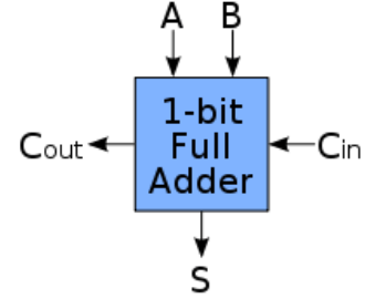
Full Adder:
1-bit Full Adder
A 1-bit Full Adder is a combinational circuit that adds three binary inputs (A, B, and Cin) and produces two outputs: Sum (S) and Carry-out (Cout). It's the fundamental building block for multi-bit addition operations.
Block Diagram
Internal Logic Design
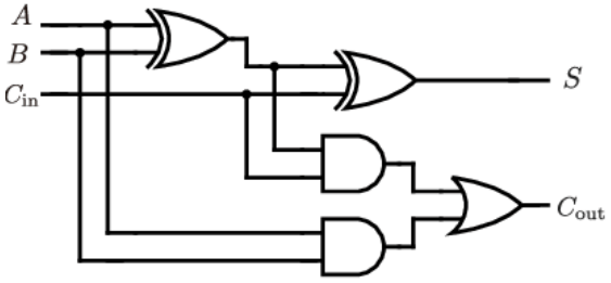
Logic Implementation:
- Sum (S): Generated using two XOR gates: S = A ⊕ B ⊕ Cin
- Carry-out (Cout): Generated using AND and OR gates: Cout = (A·B) + (A⊕B)·Cin
- Propagation: Carry ripples through the circuit based on input combinations
Truth Table
| A | B | Cin | S | Cout |
|---|---|---|---|---|
| 0 | 0 | 0 | 0 | 0 |
| 0 | 0 | 1 | 1 | 0 |
| 0 | 1 | 0 | 1 | 0 |
| 0 | 1 | 1 | 0 | 1 |
| 1 | 0 | 0 | 1 | 0 |
| 1 | 0 | 1 | 0 | 1 |
| 1 | 1 | 0 | 0 | 1 |
| 1 | 1 | 1 | 1 | 1 |
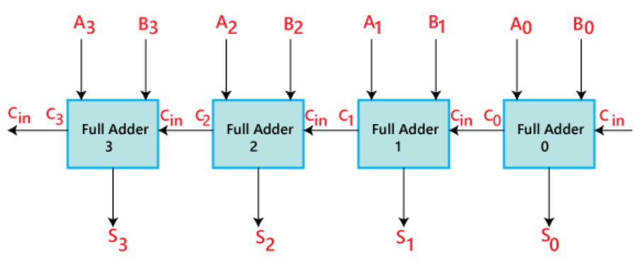
4-bit Parallel Adder
A 4-bit Parallel Adder is constructed by cascading four 1-bit Full Adders together, where the Carry-out of each stage becomes the Carry-in of the next stage. This enables parallel processing of multi-bit binary numbers.
Key Features
- Parallel Processing: All bits are processed simultaneously for faster operation
- Carry Propagation: Carry ripples through each stage sequentially (ripple carry)
- Scalable Design: Can be extended to any number of bits (8-bit, 16-bit, 32-bit)
- Standard IC: Available as 7483 (4-bit full adder) or 74283 with enhanced features
- Applications: Arithmetic logic units (ALUs), calculators, digital signal processors
Operation Principle
The 4-bit parallel adder operates by:
- Receiving two 4-bit binary numbers (A3A2A1A0 and B3B2B1B0)
- Processing each bit pair through individual full adders
- Propagating carry from least significant bit (LSB) to most significant bit (MSB)
- Generating a 4-bit sum (S3S2S1S0) and final carry-out
Pre-lab Activity:
Circuit Design Task: Sketch the logic and circuit diagrams for the BCD-to-Excess-3 converter using the 4-bit full adder (7483/74283).
Requirements:
- Design the complete circuit diagram showing all connections
- Label all inputs, outputs
- Include the 4-bit full adder IC with proper pin connections
- Show the BCD input (4 bits) and Excess-3 output (4 bits)
- Indicate the constant addition of 0011 (binary 3) to BCD input
BCD to Excess-3 Converter Simulator
BCD Input (WXYZ)
Decimal: 0
Conversion Logic: Excess-3 = BCD + 0011
7-Segment Displays
Decimal: 3
Excess-3 Binary Output LEDs
4-bit Full Adder IC Pin Configurations
7483 4-bit Full Adder
The 7483 is a 4-bit binary full adder with fast carry lookahead. It features four full-adder stages with internal carry lookahead for high-speed operation.
Key Features:
- Package: 16-pin DIP
- Supply Voltage: 4.75V to 5.25V
- Propagation Delay: 15ns typical
- Temperature Range: 0°C to 70°C
Lab 8: Using Decoders
Objectives:
Becoming familiar with decoders
Experiments Requirements:
This experiment uses the following TTL level ICs:
Procedure:
- Design the circuit with a decoder and external gates, for the combinational circuit which is defined as follows:
F1 = x'y'z' + xzF2 = xy'z' + x'yF3 = x'y'z' + xy
Understanding Decoders:
General Decoder Block Diagram
General Decoder Block Diagram
Decoder Fundamentals
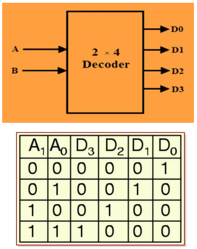
A decoder is a combinational logic circuit that converts binary information from n input lines to a maximum of 2n unique output lines. The decoder activates exactly one output line based on the binary value of the input combination, while all other outputs remain inactive.
Key Characteristics
- Input-Output Relationship: n inputs generate 2n outputs (where n is the number of input bits)
- One-Hot Output: Only one output is active (typically HIGH) at any given time
- Binary Decoding: Input binary value determines which specific output line is activated
- Enable Control: Many decoders include enable inputs for output control and cascading
Common Decoder Configurations
- 2-to-4 Decoder (74139): 2 inputs → 4 outputs (22 = 4)
- 3-to-8 Decoder (74LS238): 3 inputs → 8 outputs (23 = 8)
- 4-to-16 Decoder: 4 inputs → 16 outputs (24 = 16)
- n-to-2n Decoder: n inputs → 2n outputs
Applications
Decoders are commonly used in:
- Address Decoding: Memory and I/O address selection in computer systems
- Instruction Decoding: CPU instruction interpretation and control signal generation
- Display Control: 7-segment display and LED matrix control
- Function Generation: Implementing Boolean functions using decoder outputs and OR gates
- Data Demultiplexing: Routing data to specific output channels
Pre-lab Activity:
1. Use boolean Algebric rules to reach for mean terms of the 3 functions (F1, F2, and F3):
Apply Boolean algebra rules to find the minterms for the three functions:
2. Use Truth table for three functions (F1, F2, and F3) to reach for mean terms:
| Z | Y | X | F1 | F2 | F3 |
|---|---|---|---|---|---|
| 0 | 0 | 0 | |||
| 0 | 0 | 1 | |||
| 0 | 1 | 0 | |||
| 0 | 1 | 1 | |||
| 1 | 0 | 0 | |||
| 1 | 0 | 1 | |||
| 1 | 1 | 0 | |||
| 1 | 1 | 1 |
Write the three functions as sum of mean terms (ex: Fx = ∑(𝑚i , ..)):
3. Design the circuit with a decoder and external gates for three functions (F1, F2, and F3):
IC 74283 4-bit Full Adder Pin Configuration
IC 74283 4-bit Full Adder
The 74283 is a 4-bit binary full adder with fast carry lookahead. It features four full-adder stages with internal carry lookahead for high-speed operation, making it ideal for implementing the three functions (F1, F2, and F3) using decoder outputs and external gates.
Key Features:
- Package: 16-pin DIP
- Supply Voltage: 4.75V to 5.25V
- Propagation Delay: 15ns typical
- Temperature Range: 0°C to 70°C
- Inputs: A4, A3, A2, A1 (4-bit binary number A)
- Inputs: B4, B3, B2, B1 (4-bit binary number B)
- Input: C0 (Carry input)
- Outputs: Σ4, Σ3, Σ2, Σ1 (4-bit sum)
- Output: C4 (Carry output)
Detailed Solution Explanation:
Implementation Strategy:
Using IC 74283 with Decoder and External Gates:
- Decoder Selection: Choose appropriate decoder (74139 for 2x4 or 74LS138/74LS238 for 3x8)
- Input Mapping: Map input variables (Z, Y, X) to decoder inputs
- Output Selection: Use decoder outputs to select specific minterms for each function
- External Gates: Combine decoder outputs with OR gates to implement F1, F2, and F3
Important Note:
If you are going to use 74LS138 IC, the truth table of it is converted as ones becomes zeros and vice versa for output.
This means that for the 74LS138 decoder:
- When input combination is active, the corresponding output is LOW (0)
- All other outputs remain HIGH (1)
- This is the opposite behavior of standard decoders where active outputs are HIGH
- Consider this inversion when designing your external gate connections
Boolean Algebra Solution
Your Answer:
Correct Answer:
Sum of Mean Terms Answer
Your Answer:
Correct Answer:
Sum of minterms:
F1 = ∑(𝑚₀ , 𝑚₅ , 𝑚₇)
F2 = ∑(𝑚₁ , 𝑚₂ , 𝑚₆)
F3 = ∑(𝑚₀ , 𝑚₃ , 𝑚₇)
Detailed Solution Explanation:
1) F1 = ∑(𝑚₀ , 𝑚₅ , 𝑚₇):
- 𝑚₀ (000): F1 = 1
- 𝑚₅ (101): F1 = 1
- 𝑚₇ (111): F1 = 1
These minterms represent the input combinations where F1 equals 1 based on the truth table results above.
2) F2 = ∑(𝑚₁ , 𝑚₂ , 𝑚₆):
- 𝑚₁ (001): F2 = 1
- 𝑚₂ (010): F2 = 1
- 𝑚₆ (110): F2 = 1
These minterms represent the input combinations where F2 equals 1 based on the truth table results above.
3) F3 = ∑(𝑚₀ , 𝑚₃ , 𝑚₇):
- 𝑚₀ (000): F3 = 1
- 𝑚₃ (011): F3 = 1
- 𝑚₇ (111): F3 = 1
These minterms represent the input combinations where F3 equals 1 based on the truth table results above.
4) Summary:
The correct answer is based on the truth table results above:
Each function F1, F2, and F3 is expressed as a sum of minterms where the function equals 1. The minterms are determined by analyzing the truth table and identifying which input combinations (Z, Y, X) produce an output of 1 for each function.
3x8 Decoder with OR Gates Simulator
D4: 0 | D5: 0 | D6: 0 | D7: 0
Decoder Examples
Logic Design: 3x8 Decoder with External Gates

Logic Design Implementation
This diagram shows the complete logic design for implementing the three functions (F1, F2, and F3) using a 3x8 decoder and external OR gates. The design demonstrates how decoder outputs are combined to create the desired Boolean functions.
Design Components:
- 3x8 Decoder: Converts 3-bit binary input (Z, Y, X) to 8 active-low outputs
- External OR Gates: Combine specific decoder outputs for each function
- External NOT Gates: In order to invert active-low of 74138 IC
- Function F1: D0 + D5 + D7 (sum of minterms 0, 5, and 7)
- Function F2: D1 + D2 + D6 (sum of minterms 1, 2, and 6)
- Function F3: D0 + D3 + D7 (sum of minterms 0, 3, and 7)
Important Implementation Note:
Decoder IC Selection:
If you use 74238 IC instead of 74138:
- 74138 (Active-Low): Outputs are active-low (LOW when selected, HIGH when not selected)
- 74238 (Active-High): Outputs are active-high (HIGH when selected, LOW when not selected)
- Design Modification: For 74238, simply remove the NOT gates from the above logic design
- Connection: Connect decoder outputs directly to OR gate inputs without inversion
- Result: The same logical functions (F1, F2, F3) will be achieved with simpler gate connections
Implementation Summary:
Current Design (74138): Uses active-low outputs with NOT gates for proper logic
Alternative Design (74238): Remove NOT gates and connect outputs directly to OR gates
Both Designs: Produce identical function outputs (F1, F2, F3) with different gate configurations
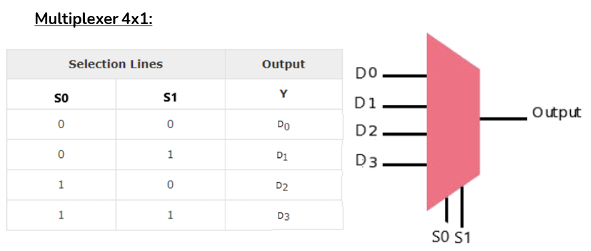
Lab 9: Using Multiplexers
Objectives:
Becoming familiar with multiplexer and full adders
Experiments Requirements:
This experiment uses the following TTL level ICs:
Procedure:
- Implement the following Boolean function with 8*1 multiplexer
F(A,B,C,D) = Σ(0,3,4,7,8,9,12,15)
Understanding Multiplexer / Demultiplexer:
Multiplexer:
General Multiplexer Block Diagram
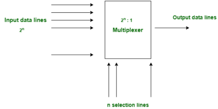
Definition
A multiplexer is a data selector which takes several inputs and gives a single output. In multiplexer we have 2n input lines and 1 output lines where n is the number of selection lines.
Key Characteristics
- Input-Output Relationship: 2n inputs generate 1 output (where n is the number of selection bits)
- Data Selection: Selection lines determine which input is routed to the output
- Single Output: Only one input is selected and routed to the output at any given time
- Enable Control: Many multiplexers include enable inputs for output control and cascading
Common Multiplexer Configurations
- 2-to-1 Multiplexer: 2 inputs → 1 output (21 = 2)
- 4-to-1 Multiplexer: 4 inputs → 1 output (22 = 4)
- 8-to-1 Multiplexer (74151): 8 inputs → 1 output (23 = 8)
- 16-to-1 Multiplexer: 16 inputs → 1 output (24 = 16)
Applications
Multiplexers are commonly used in:
- Data Routing: Selecting data from multiple sources to a single destination
- Address Multiplexing: Sharing address lines between different memory banks
- Function Implementation: Implementing Boolean functions using multiplexer inputs
- Data Transmission: Combining multiple data streams into a single channel
- Control Systems: Selecting control signals from multiple sources
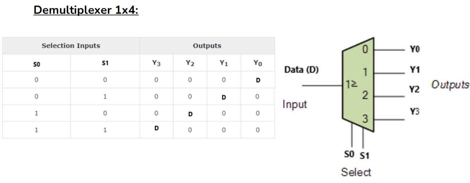
Demultiplexer:
General Demultiplexer Block Diagram
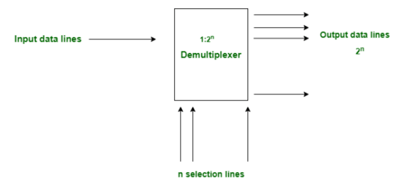
Definition
A demultiplexer is a data distributor which takes a single input and gives several outputs. In demultiplexer we have 1 input and 2n output lines where n is the selection line.
Key Characteristics
- Input-Output Relationship: 1 input generates 2n outputs (where n is the number of selection bits)
- Data Distribution: Selection lines determine which output receives the input data
- Single Input: Only one input is distributed to one of the multiple outputs at any given time
- Enable Control: Many demultiplexers include enable inputs for output control and cascading
Common Demultiplexer Configurations
- 1-to-2 Demultiplexer: 1 input → 2 outputs (21 = 2)
- 1-to-4 Demultiplexer: 1 input → 4 outputs (22 = 4)
- 1-to-8 Demultiplexer: 1 input → 8 outputs (23 = 8)
- 1-to-16 Demultiplexer: 1 input → 16 outputs (24 = 16)
Applications
Demultiplexers are commonly used in:
- Data Distribution: Routing data from one source to multiple destinations
- Memory Address Decoding: Selecting specific memory locations or banks
- Display Control: Controlling multiple displays or LED segments from a single source
- Signal Routing: Directing control signals to different subsystems
- Communication Systems: Broadcasting data to multiple receivers
Pre-lab Activity:
1. Fill the following truth table for the function:
Implementation Strategy
Objective
Implement the Boolean function F(A,B,C,D) = ∑(0,3,4,7,8,9,12,15) using only one 8×1 Multiplexer (MUX).
Strategy
Use A, B, C as selection lines and analyze D's influence on consecutive outputs. For each pair of consecutive rows (D=0, D=1), determine the optimal input to the MUX data lines.
MUX Input Options
Each MUX data line can receive: 0, 1, D, or D' based on the pattern analysis of F outputs.
| A | B | C | D | F | MUX Input |
|---|---|---|---|---|---|
| 0 | 0 | 0 | 0 | ||
| 0 | 0 | 0 | 1 | ||
| 0 | 0 | 1 | 0 | ||
| 0 | 0 | 1 | 1 | ||
| 0 | 1 | 0 | 0 | ||
| 0 | 1 | 0 | 1 | ||
| 0 | 1 | 1 | 0 | ||
| 0 | 1 | 1 | 1 | ||
| 1 | 0 | 0 | 0 | ||
| 1 | 0 | 0 | 1 | ||
| 1 | 0 | 1 | 0 | ||
| 1 | 0 | 1 | 1 | ||
| 1 | 1 | 0 | 0 | ||
| 1 | 1 | 0 | 1 | ||
| 1 | 1 | 1 | 0 | ||
| 1 | 1 | 1 | 1 |
2. Design the circuit with 8×1 multiplexer for F(A,B,C,D):
8×1 Multiplexer (74151) Pin Configuration
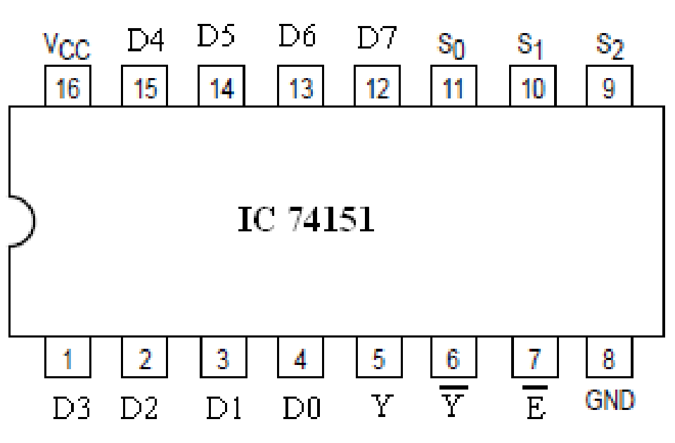
8×1 Multiplexer (74151)
The 74151 is an 8-to-1 line data selector/multiplexer with complementary outputs. It features three binary select inputs (A, B, C) and eight data inputs (D0-D7), making it ideal for implementing the function F(A,B,C,D) using A, B, C as selection lines and D as the data input.
Key Features:
- Package: 16-pin DIP
- Supply Voltage: 4.75V to 5.25V
- Propagation Delay: 15ns typical
- Temperature Range: 0°C to 70°C
- Select Inputs: A, B, C (3-bit binary selection)
- Data Inputs: D0-D7 (8 data input lines)
- Outputs: Y (selected data output), W (complementary output)
- Enable: G (active LOW enable input)
Implementation Strategy:
8×1 MUX Implementation:
Using 74151 8×1 Multiplexer:
- Selection Lines: Connect A, B, C to the select inputs (A, B, C)
- Data Lines: Connect D0-D7 based on MUX Input analysis from truth table
- Data Inputs: Each data line receives 0, 1, D, or D' as determined
- Output: Y output provides the function F(A,B,C,D)
Important Note:
The MUX Input column in the truth table determines what connects to each data line:
- 0: Connect to ground (0V)
- 1: Connect to VCC (+5V)
- D: Connect to input variable D
- D': Connect to inverted input variable D (use NOT gate)
8×1 Multiplexer Simulator
A, B, C are selectors, D is data input
D4: 0 | D5: 0 | D6: 0 | D7: 0
Multiplexer Examples
Demultiplexer Examples
Logic Design: 8×1 Multiplexer Implementation

Logic Design Implementation
This diagram shows the complete logic design for implementing the function F(A,B,C,D) = ∑(0,3,4,7,8,9,12,15) using an 8×1 multiplexer. The design demonstrates how the multiplexer data inputs are configured to achieve the desired Boolean function.
Design Components:
- 8×1 Multiplexer: Uses A, B, C as selection lines and D as data input
- Data Input Configuration: Each data line (D0-D7) is connected based on the truth table analysis
- Selection Logic: A, B, C combinations select the appropriate data input
- Data Input D: The variable D is used as input to create the required function
- Function F(A,B,C,D): Implements the sum of minterms 0, 3, 4, 7, 8, 9, 12, 15
Important Implementation Note:
Data Input Strategy:
Based on the truth table analysis:
- D0 (A=0,B=0,C=0): Connected to D' (inverted D) - Pattern: F(0,0,0,0)=1, F(0,0,0,1)=0
- D1 (A=0,B=0,C=1): Connected to D - Pattern: F(0,0,1,0)=0, F(0,0,1,1)=1
- D2 (A=0,B=1,C=0): Connected to D' - Pattern: F(0,1,0,0)=1, F(0,1,0,1)=0
- D3 (A=0,B=1,C=1): Connected to D - Pattern: F(0,1,1,0)=0, F(0,1,1,1)=1
- D4 (A=1,B=0,C=0): Connected to 1 (VCC) - Pattern: F(1,0,0,0)=1, F(1,0,0,1)=1
- D5 (A=1,B=0,C=1): Connected to 0 (Ground) - Pattern: F(1,0,1,0)=0, F(1,0,1,1)=0
- D6 (A=1,B=1,C=0): Connected to D' - Pattern: F(1,1,0,0)=1, F(1,1,0,1)=0
- D7 (A=1,B=1,C=1): Connected to D - Pattern: F(1,1,1,0)=0, F(1,1,1,1)=1
Implementation Summary:
Multiplexer Configuration: A, B, C serve as selection lines (000 to 111)
Data Inputs: D0=D', D1=D, D2=D', D3=D, D4=1, D5=0, D6=D', D7=D
Result: The multiplexer output will be HIGH only for the specified minterms, implementing F(A,B,C,D) = ∑(0,3,4,7,8,9,12,15)
Lab 10: Flip Flops
Objectives:
Becoming familiar with flip flops such as D-flip flop, JK-flip flop. How to connect clock from the kit IC
Experiments Requirements:
This experiment uses the following TTL level ICs:
Understanding JK-Flip Flop/ D-Flip Flop:
D-Flip Flop:
General D-Flip Flop Block Diagram
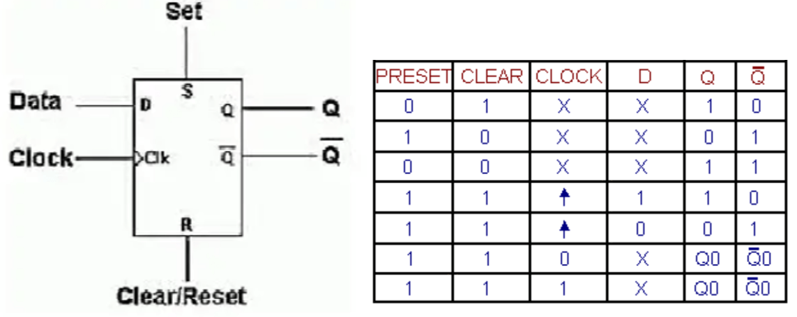
Definition
A D-Flip Flop is a sequential logic device that stores one bit of data. The output Q follows the input D when a clock pulse is applied, making it a fundamental building block for memory and sequential circuits.
Key Characteristics
- Data Storage: Stores the value of D input at the rising edge of the clock
- Clock-Triggered: Output changes only on clock edge, not continuously
- Single Data Input: One data input (D) determines the next state
- Stable Output: Output remains stable between clock pulses
Common D-Flip Flop Configurations
- Positive Edge-Triggered: Changes state on rising edge of clock signal
- Negative Edge-Triggered: Changes state on falling edge of clock signal
- Master-Slave: Two-stage design for improved noise immunity
- Asynchronous Reset: Direct reset capability independent of clock
Applications
D-Flip Flops are commonly used in:
- Data Registers: Storing multiple bits of data in parallel
- Counters: Building sequential counting circuits
- Memory Elements: Basic storage units in digital systems
- State Machines: Implementing sequential logic circuits
- Data Synchronization: Aligning data with clock signals
JK-Flip Flop:
General JK-Flip Flop Block Diagram
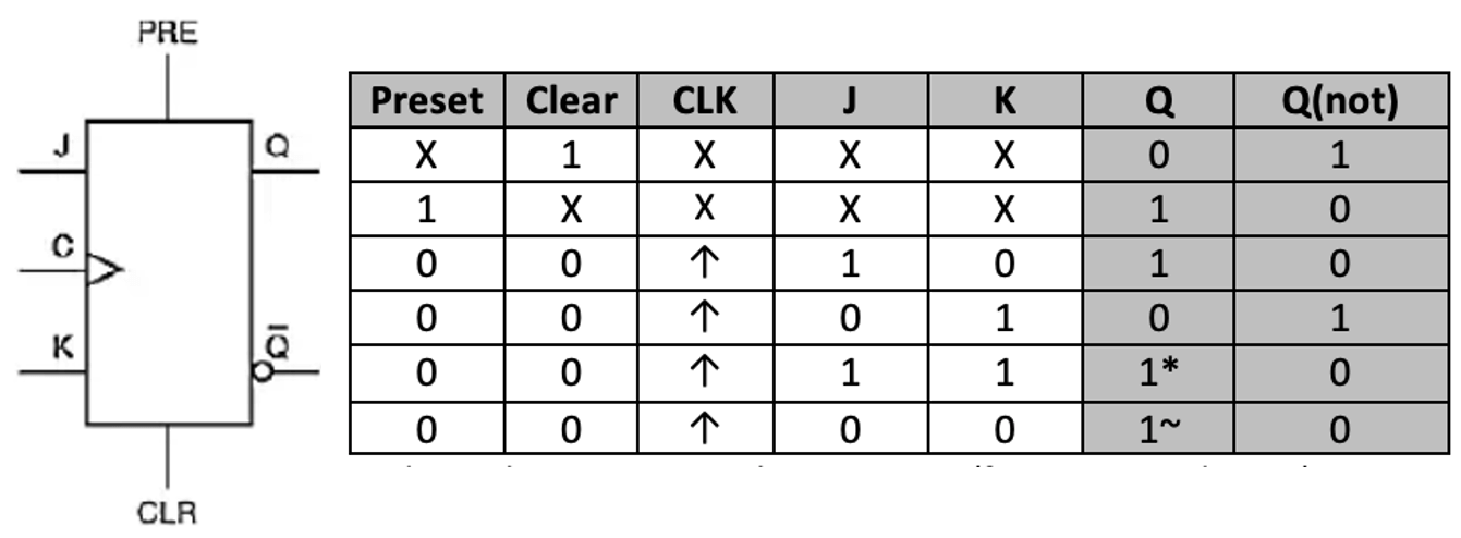
Definition
A JK-Flip Flop is a versatile sequential logic device that can perform multiple functions based on J and K inputs. It can be configured to act as a D-Flip Flop, T-Flip Flop, or maintain its current state.
Key Characteristics
- Dual Control Inputs: J and K inputs provide flexible control over output behavior
- Toggle Functionality: Can toggle output state when J=K=1
- Hold State: Maintains current output when J=K=0
- Clock-Triggered: Changes occur only on clock edge transitions
Common JK-Flip Flop Configurations
- J=0, K=0: No change (hold current state)
- J=0, K=1: Reset (Q = 0)
- J=1, K=0: Set (Q = 1)
- J=1, K=1: Toggle (Q = Q')
Applications
JK-Flip Flops are commonly used in:
- Frequency Dividers: Dividing clock frequency by 2
- Counters: Building various counting sequences
- Shift Registers: Moving data through sequential stages
- State Machines: Implementing complex sequential logic
- Memory Systems: Building reliable storage circuits
D-Flip Flop Simulation Screenshots
JK-Flip Flop Simulation Screenshots
Steps:
General Steps:
Flip Flop Implementation Process
- Power Setup:
- Connect Vcc (+5V) and GND (0V) to power rails
- Verify stable power supply before proceeding
- IC Placement:
- Insert IC into breadboard with proper orientation
- Ensure all pins are properly seated
- Input Connections:
- Connect logic switches to input pins (J, K, D, Clock)
- Connect Clear/Reset signals for initialization
- Output Monitoring:
- Connect LEDs to Q and Q̅ output pins
- Clock Connection:
- Connect clock signal from kit generator
- Use manual button for single-step testing
- Testing Sequence:
- Initialize with Clear/Reset signal
- Apply input combinations and observe outputs
- Verify behavior matches truth table
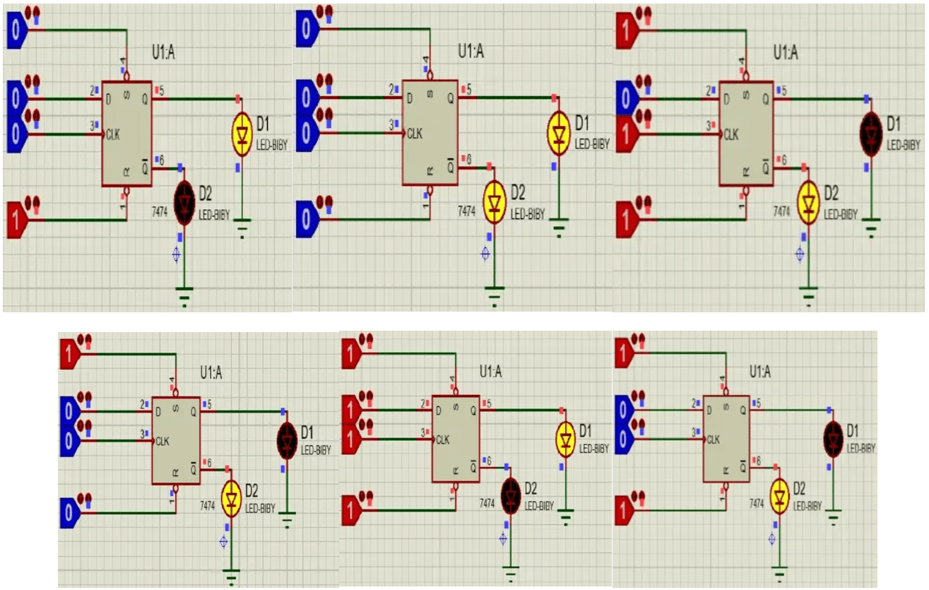
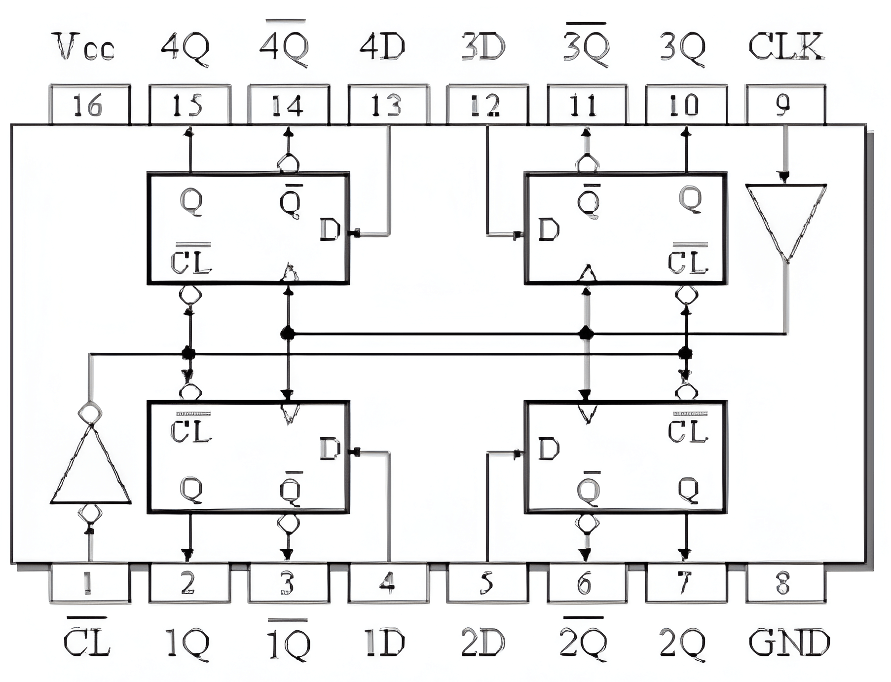
D Flip-Flop (74175) IC:
- Testing Procedure:
- Set CLR̅ = LOW briefly to clear Q=0, Q̅=1
- Set CLR̅ = HIGH, PRE̅ = HIGH for normal operation
- Apply D input and clock pulse: Q follows D at rising edge
- Test: D=0→Q=0, D=1→Q=1 after clock pulse
74175 D-Flip Flop Pin Configuration
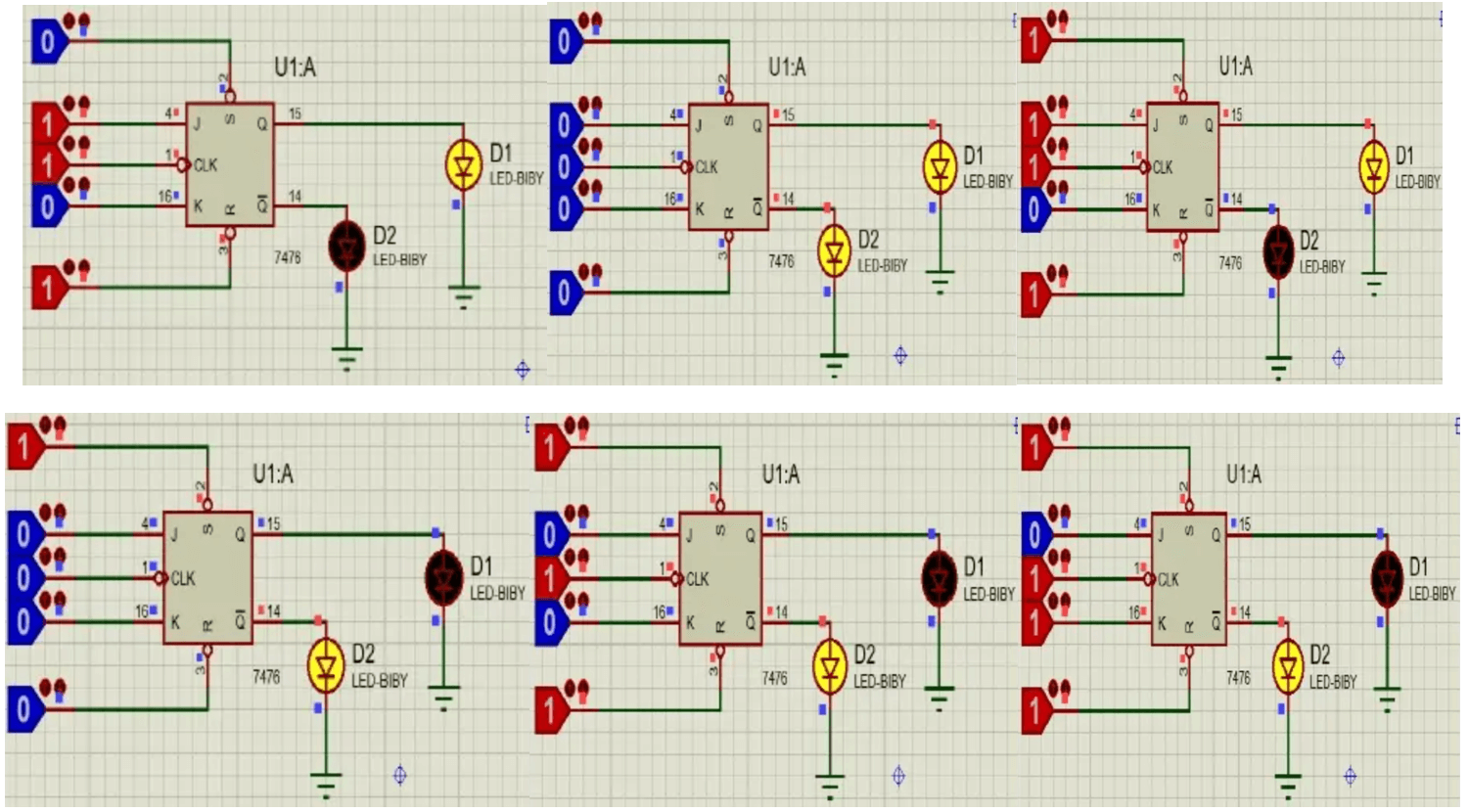
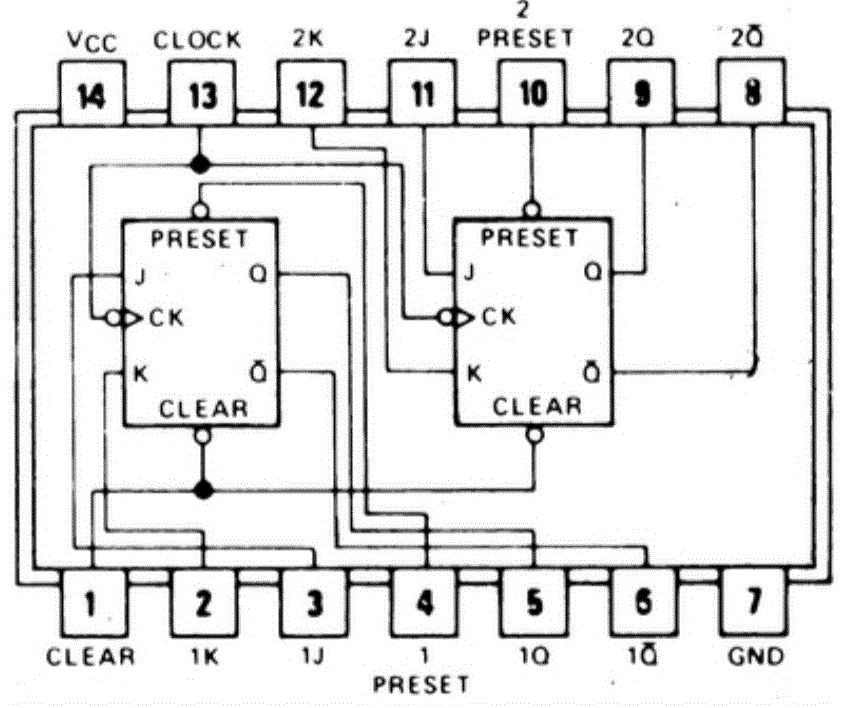
JK Flip-Flop (74114) IC:
- Testing Procedure:
- Set CLR̅ = LOW briefly to clear Q=0, Q̅=1
- Set CLR̅ = HIGH, PRE̅ = HIGH for normal operation
- Test truth table: J=0,K=0 (hold), J=0,K=1 (reset), J=1,K=0 (set), J=1,K=1 (toggle)
74114 JK-Flip Flop Pin Configuration
Flip Flop Simulator
Clock Signal Generator
Choose Simulator
D Flip Flop (74175) Simulator
JK Flip Flop (74114) Simulator
MOD-7 Counter Simulator
Purpose: Simulates a 3-bit MOD-7 counter using JK Flip Flops with external gates.
Counter Sequence:
- Binary: 000 → 001 → 010 → 011 → 100 → 101 → 110 → 000
- Decimal: 0 → 1 → 2 → 3 → 4 → 5 → 6 → 0
- Cycle: Repeats indefinitely with clock pulses
Components:
- 3 JK Flip Flops: A (MSB), B, C (LSB)
- External Gates: Combinational logic for next state
- Clock Signal: Synchronizes all transitions
- 7-Segment Display: Shows decimal output
Operation:
- Clock rising edge triggers state change
- JK inputs determine next state based on current state
- Binary outputs drive 7-segment display
- Debug logger shows internal JK states
D Flip Flop (74175) Simulator
IC 74175: Quad D-type flip flop with clear and preset capabilities.
Operation Modes:
- Asynchronous Clear (CLR̅): Immediate reset when active LOW
- Asynchronous Preset (PRE̅): Immediate set when active LOW
- Synchronous Data: Q follows D at clock rising edge
- Normal Operation: Maintains current state
Setup Time Violation:
Occurs when D input changes during the setup time window before the clock rising edge. This is normal behavior that simulates real IC timing requirements.
Truth Table:
| CLR̅ | PRE̅ | CLK | D | Q | Q̅ |
|---|---|---|---|---|---|
| 0 | X | X | X | 0 | 1 |
| X | 0 | X | X | 1 | 0 |
| 1 | 1 | ↑ | 0 | 0 | 1 |
| 1 | 1 | ↑ | 1 | 1 | 0 |
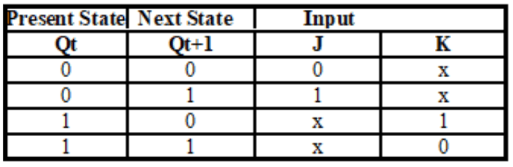
JK Flip Flop (74114) Simulator
IC 74114: Dual JK flip flop with clear and preset capabilities.
Operation Modes:
- Hold (J=0, K=0): Maintains current state
- Reset (J=0, K=1): Sets Q = 0, Q̅ = 1
- Set (J=1, K=0): Sets Q = 1, Q̅ = 0
- Toggle (J=1, K=1): Q changes to opposite state
Truth Table:
| CLR̅ | PRE̅ | CLK | J | K | Q | Q̅ |
|---|---|---|---|---|---|---|
| 0 | X | X | X | X | 0 | 1 |
| X | 0 | X | X | X | 1 | 0 |
| 1 | 1 | ↑ | 0 | 0 | Q | Q̅ |
| 1 | 1 | ↑ | 0 | 1 | 0 | 1 |
| 1 | 1 | ↑ | 1 | 0 | 1 | 0 |
| 1 | 1 | ↑ | 1 | 1 | Q̅ | Q |
Key Features:
- Versatile Operation: Four distinct modes of operation
- Toggle Mode: Useful for frequency division and counting
- Asynchronous Control: Immediate clear/preset regardless of clock
- Setup Time: J,K inputs must be stable before clock edge
Clock Signal Generator
Purpose: Generates digital clock signals for flip flop simulation and testing.
Frequency Options:
- 0.5 Hz (Slow): 2-second period, ideal for detailed observation
- 1 Hz (Normal): 1-second period, standard simulation speed
- 2 Hz (Fast): 0.5-second period, faster operation
- 5 Hz (Very Fast): 0.2-second period, rapid testing
Control Functions:
- Start Clock: Begins continuous clock signal generation
- Stop Clock: Halts clock signal generation
- Single Pulse: Generates one complete clock cycle
- Reset Flip Flops: Clears all flip flop states to initial values
Clock Signal Characteristics:
- Square Wave: Digital signal with sharp transitions
- 50% Duty Cycle: Equal HIGH and LOW periods
- Rising Edge: Positive transition (LOW to HIGH)
- Falling Edge: Negative transition (HIGH to LOW)
Visual Indicators:
- Waveform Display: Real-time visual representation of clock signal
- State Indicator: Shows current clock level (HIGH/LOW)
- Edge Indicator: Displays current transition type
- Color Coding: Visual feedback for signal state changes
Key Features:
- Variable Frequency: Adjustable clock speed for different testing needs
- Real-time Control: Immediate start/stop functionality
- Single Pulse Mode: Step-by-step analysis capability
- Synchronized Operation: All flip flops respond to same clock signal
- Visual Feedback: Clear indication of clock state and transitions
Lab 11: Using Counters
Objectives:
How to use counter IC and how to design counter with a specific count
Experiments Requirements:
This experiment uses the following TTL level ICs; the pin configurations for these ICs are available in appendix A:
Procedure:
- Design a counter with the following binary repeated sequence: 0, 1, 2, 3, 4, 5, 6 using JK flip-flops and external gates
Pre-lab Activity:
1. Fill the following truth table for designing of counter using 3 JK flip-flops:
Note that To build the truth table of the MOD-7 counter, first list the present state (A,B,C) and its next state according to the sequence 0→1→2→3→4→5→6→0, then—based on the following truth table of the JK flip-flop—determine the required inputs (JA–KA, JB–KB, JC–KC) for each transition.
| A | B | C | JA | KA | JB | KB | JC | KC |
|---|---|---|---|---|---|---|---|---|
| 0 | 0 | 0 | ||||||
| 0 | 0 | 1 | ||||||
| 0 | 1 | 0 | ||||||
| 0 | 1 | 1 | ||||||
| 1 | 0 | 0 | ||||||
| 1 | 0 | 1 | ||||||
| 1 | 1 | 0 |
2. Simplify (JA - KA - JB - KB - JC - KC) using K-maps:
Choose K-Map
JA K-Map:
Write the simplified expression:
KA K-Map:
Write the simplified expression:
JB K-Map:
Write the simplified expression:
KB K-Map:
Write the simplified expression:
JC K-Map:
Write the simplified expression:
KC K-Map:
Write the simplified expression:
JA K-Map Simplification Answer
Your K-Map Values:
Your Simplified Expression:
Correct K-Map Values:
Note: Yellow highlighted X in A-BC column (row 1, col 2) is chosen as 1 for simplification
Correct Simplified Expression:
JA = BC
Detailed Solution Explanation:
1) Analyze the K-Map for JA
Looking at the K-Map, we can see that JA = 1 when:
- A'-BC = 1 (definite 1)
- A-BC = X (don't care, chosen as 1)
The X in A-BC column is chosen as 1 to optimize the expression.
2) Group the 1's
We can form one group covering the BC column:
- Group: BC (covers A'-BC and A-BC)
This group covers both the definite 1 and the chosen X.
3) Write the simplified expression
JA = BC
This is the minimal form since the BC column covers all 1's when X is chosen as 1.
KA K-Map Simplification Answer
Your K-Map Values:
Your Simplified Expression:
Correct K-Map Values:
Note: Yellow highlighted X's in A' row (BC' and BC columns) & A row (BC column) are chosen as 1 for simplification
Correct Simplified Expression:
KA = B
Detailed Solution Explanation:
1) Analyze the K-Map for KA
Looking at the K-Map, we can see that KA = 1 when:
- A-BC' = 1 (definite 1)
- A'-BC' = X (don't care, chosen as 1)
- A'-BC = X (don't care, chosen as 1)
- A-BC = X (don't care, chosen as 1)
2) Group the 1's
We can form one group covering the entire B column:
- Group: B (covers A'-BC', A'-BC, A-BC', and A-BC)
This group covers the definite 1 and both chosen X's.
3) Write the simplified expression
KA = B
This is the minimal form since the B column covers all 1's when the X's are chosen as 1.
JB K-Map Simplification Answer
Your K-Map Values:
Your Simplified Expression:
Correct K-Map Values:
Note: Yellow highlighted X's in BC column (both rows) are chosen as 1 for simplification
Correct Simplified Expression:
JB = C
Detailed Solution Explanation:
1) Analyze the K-Map for JB
Looking at the K-Map, we can see that JB = 1 when:
- A-B'C = 1 (definite 1)
- A'-B'C = 1 (definite 1)
- A-BC = X (don't care, chosen as 1)
- A'-BC = X (don't care, chosen as 1)
The 2 X's in the BC column are chosen as 1 to optimize the expression.
2) Group the 1's
We can form one group covering the entire C column:
- Group: C (covers A'-BC, A-BC, A-B'C, and A'-B'C)
This group covers the definite 1 and both chosen X's.
3) Write the simplified expression
JB = C
This is the minimal form since the C column covers all 1's when the X's are chosen as 1.
KB K-Map Simplification Answer
Your K-Map Values:
Your Simplified Expression:
Correct K-Map Values:
Note: Yellow highlighted X's in A row (B'C', B'C, BC columns) and A' row (B'C column) are chosen as 1 for simplification
Correct Simplified Expression:
KB = C + A
Detailed Solution Explanation:
1) Analyze the K-Map for KB
Looking at the K-Map, we can see that KB = 1 when:
- A'-BC = 1 (definite 1)
- A'-B'C = X (don't care, chosen as 1)
- A-B'C' = X (don't care, chosen as 1)
- A-B'C = X (don't care, chosen as 1)
- A-BC = X (don't care, chosen as 1)
- A-BC' = 1 (definite 1)
The 3 X's in the A row and 1 X in the A' row are chosen as 1 to optimize the expression.
2) Group the 1's
We can form two groups:
- Group 1: C (covers A-B'C, A'-B'C, A-BC, and A-BC)
- Group 2: A (covers A-B'C', A-B'C, A-BC, and A-BC')
These groups cover all the 1's when the X's are chosen as 1.
3) Write the simplified expression
KB = C + A
This is the minimal form since the C group and A group cover all 1's when the X's are chosen as 1.
JC K-Map Simplification Answer
Your K-Map Values:
Your Simplified Expression:
Correct K-Map Values:
Note: Yellow highlighted X's in B'C column (both A' and A rows) and BC column (both A' and A rows) are chosen as 1 for simplification
Correct Simplified Expression:
JC = A' + B'
Detailed Solution Explanation:
1) Analyze the K-Map for JC
Looking at the K-Map, we can see that JC = 1 when:
- A'-B'C' = 1 (definite 1)
- A-B'C' = 1 (definite 1)
- A'-B'C = X (don't care, chosen as 1)
- A-B'C = X (don't care, chosen as 1)
- A'-BC = X (don't care, chosen as 1)
- A-BC = X (don't care, chosen as 1)
- A'-BC' = 1 (definite 1)
The 2 X's in the B'C and BC columns are chosen as 1 to optimize the expression.
2) Group the 1's
We can form two groups:
- Group 1: A' (covers A'-B'C', A'-B'C, A'-BC, and A'-BC')
- Group 2: B' (covers A'-B'C', A-B'C', A'-B'C, and A-B'C)
These groups cover all the 1's when the X's are chosen as 1.
3) Write the simplified expression
JC = A' + B'
This is the minimal form since the A' group and B' group cover all 1's when the X's are chosen as 1.
KC K-Map Simplification Answer
Your K-Map Values:
Your Simplified Expression:
Correct K-Map Values:
Note: Yellow highlighted X in A-BC Cell is chosen as 1 for simplification
Correct Simplified Expression:
KC = C
Detailed Solution Explanation:
1) Analyze the K-Map for KC
Looking at the K-Map, we can see that KC = 1 when:
- A'-B'C = 1 (definite 1)
- A-B'C = 1 (definite 1)
- A'-BC = 1 (definite 1)
- A-BC = X (don't care, chosen as 1)
The X in A-BC column is chosen as 1 to optimize the expression.
2) Group the 1's
We can form one group covering the entire C column:
- Group: C (covers A'-B'C, A-B'C, A'-BC, and A-BC)
This group covers the definite 1 and the chosen X.
3) Write the simplified expression
KC = C
This is the minimal form since the C column covers all 1's when the X is chosen as 1.
3. Design the circuit with JK-FlipFlops and external gates for a counter with the following binary repeated sequence: 0, 1, 2, 3, 4, 5, 6:
MOD-7 Counter Simulator
Clock Signal Generator
Counter State (ABC)
7-Segment Display
Binary State LEDs
Decimal: 0
JK Flip Flop Debug Logger
QA: 0 | Q̅A: 1
QB: 0 | Q̅B: 1
QC: 0 | Q̅C: 1
MOD-7 Counter Simulator
Purpose: Simulates a 3-bit MOD-7 counter using JK Flip Flops with external gates.
Counter Sequence:
- Binary: 000 → 001 → 010 → 011 → 100 → 101 → 110 → 000
- Decimal: 0 → 1 → 2 → 3 → 4 → 5 → 6 → 0
- Cycle: Repeats indefinitely with clock pulses
Components:
- 3 JK Flip Flops: A (MSB), B, C (LSB)
- External Gates: Combinational logic for next state
- Clock Signal: Synchronizes all transitions
- 7-Segment Display: Shows decimal output
Operation:
- Clock rising edge triggers state change
- JK inputs determine next state based on current state
- Binary outputs drive 7-segment display
- Debug logger shows internal JK states
Logic Design: MOD-7 Counter Implementation

Logic Design Implementation
This diagram shows the complete logic design for implementing the MOD-7 counter using JK flip-flops. The design demonstrates how the counter progresses through states 0 to 6 and then resets back to 0, creating a synchronous counting sequence.
Design Components:
- JK Flip-Flops: Three JK flip-flops (A, B, C) connected in cascade for sequential counting
- Clock Signal: Synchronous clock input that triggers state transitions on rising edge
- State Logic: Combinational logic determines next state based on current state and JK inputs
- Reset Circuit: Asynchronous reset to initialize counter to state 000
- Output Decoder: Binary-to-7-segment decoder for visual display
Counter Operation & Simulator Usage:
Counter State Sequence:
MOD-7 Counter Progression:
- State 000 (0): Initial state, counter starts here
- State 001 (1): First count, A=0, B=0, C=1
- State 010 (2): Second count, A=0, B=1, C=0
- State 011 (3): Third count, A=0, B=1, C=1
- State 100 (4): Fourth count, A=1, B=0, C=0
- State 101 (5): Fifth count, A=1, B=0, C=1
- State 110 (6): Sixth count, A=1, B=1, C=0
- State 111 (7): Reset state, counter returns to 000
Simulator Features & How to Use:
Clock Control:
- Start Clock: Begins continuous counting at selected frequency
- Stop Clock: Pauses the counting sequence
- Single Pulse: Advances counter by one clock cycle
- Reset Counter: Returns counter to initial state 000
- Frequency Control: Adjust clock speed from 0.5Hz to 5Hz
Visual Feedback:
- Binary Display: Shows current counter state in binary (ABC)
- 7-Segment Display: Visual decimal representation of count
- LED Outputs: Binary state indicators for each flip-flop
- Debug Logger: Real-time JK input and output states
Learning Objectives:
Understanding MOD-7 Counter:
- Learn synchronous sequential circuit design
- Understand JK flip-flop behavior and state transitions
- Observe binary counting sequence and overflow behavior
- Analyze clock timing and edge-triggered operations
- Practice debugging sequential circuits using visual tools